
New semiconductor projects targeting discrete devices, analog ICs and in-car displays show how India’s automotive electronics opportunity is moving closer to manufacturing.
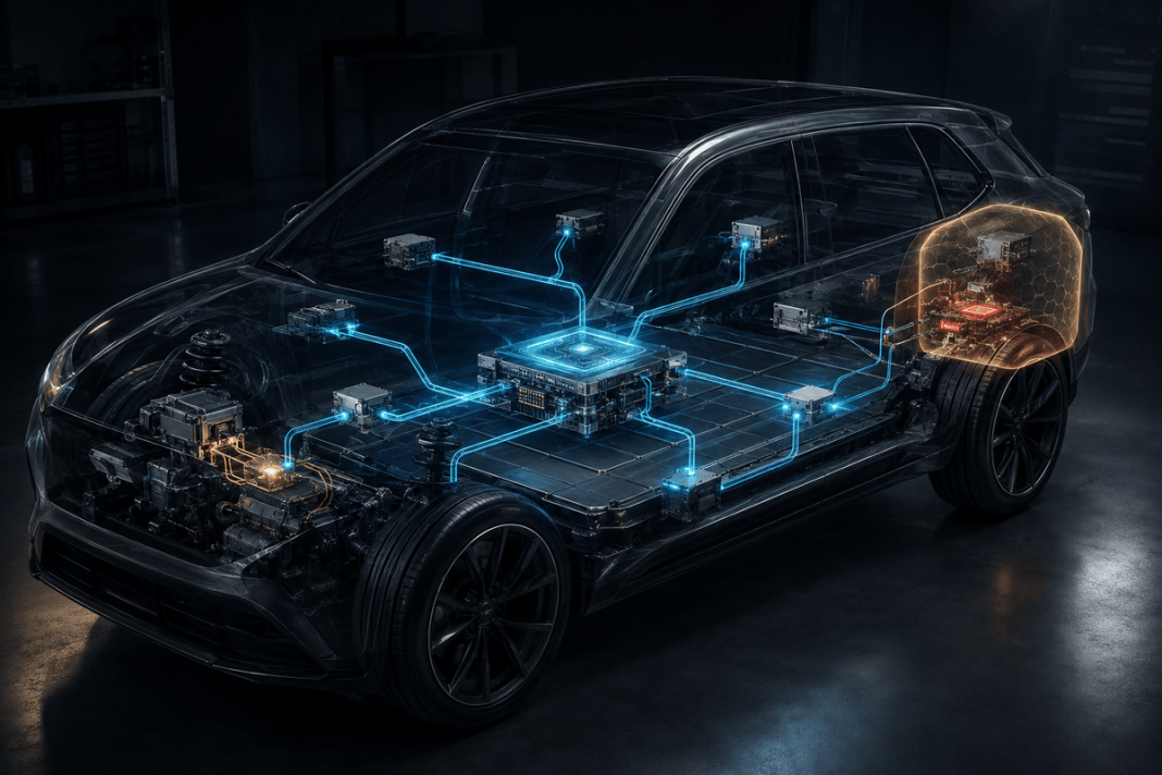
The modern vehicle is increasingly defined by semiconductors. Power devices switch energy through electric drivetrains. Analog chips measure and condition signals. Microcontrollers coordinate functions. Sensors perceive the environment, while display electronics shape the cockpit. A supply disruption in any one of these layers can slow an entire vehicle programme.
India’s semiconductor strategy is beginning to move closer to this automotive opportunity. In May 2026, the Union Cabinet approved two additional units under the India Semiconductor Mission with a combined investment of Rs 3,936 crore and an expected 2,230 skilled jobs. The approvals take the mission’s cumulative project count to 12, representing approximately Rs 1.64 lakh crore of investment.
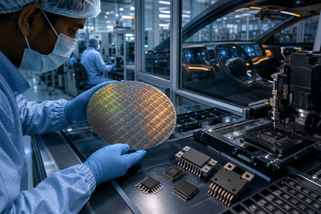
One project, proposed by Crystal Matrix in Dholera, combines a compound-semiconductor fabrication facility with assembly, testing, marking and packaging for Mini- and Micro-LED display modules. It also includes gallium nitride foundry and epitaxy capability on six-inch wafers, with in-car displays among the stated applications. The second, a Suchi Semicon facility in Surat, is an outsourced semiconductor assembly and test unit for discrete devices, with planned capacity of more than one billion chips per year across power electronics, analog ICs and industrial applications, including automotive.
Automotive semiconductor self-reliance will not come from one headline fab. It will come from a connected chain of design, fabrication, packaging, testing, qualification and high-volume manufacturing discipline.
Why Packaging and Testing Deserve Attention
Public discussion often focuses on wafer fabrication, but packaging and test are critical to automotive reliability. A semiconductor must be electrically connected, protected from the environment and verified across temperature, voltage and mechanical stress. The package influences thermal performance, parasitic electrical behaviour, footprint and long-term durability.
Automotive qualification is especially demanding because vehicles operate for years under vibration, heat, cold, moisture and electrical transients. Consistency matters across millions of parts. An OSAT facility that can build rigorous process control, traceability and customer qualification is therefore not a secondary part of the value chain; it is a core manufacturing capability.
Different GaN Applications Must Not be Confused
Gallium nitride has become strongly associated with high-efficiency power electronics, but the Dholera project’s announced automotive application includes in-car display technologies. GaN materials can support both optoelectronic and power-device use cases, yet a display-oriented compound-semiconductor line should not automatically be described as a factory for EV inverter chips. The product, process and qualification requirements are different.
This distinction matters because credible localisation depends on precision. India’s opportunity spans cockpit displays, lighting, connectivity, power management, charging, body electronics, sensing and drivetrain control. Each application requires its own device technology, packaging approach and reliability pathway. Broad claims can hide the engineering work needed to reach qualified volume.
The Automotive Opportunity is a System Opportunity
For Indian OEMs and Tier-1 suppliers, nearby semiconductor manufacturing can improve supply visibility and enable closer technical collaboration. But local availability alone is not enough. Vehicle programmes need devices designed into electronic control units, supported by development tools, validated within the system and covered by long-term supply commitments.
That creates openings for chip-design firms, packaging specialists, test-equipment companies, electronics manufacturers and automotive software teams. It also creates a need for laboratories that can support failure analysis, electromagnetic compatibility, thermal characterisation and reliability testing. Talent must bridge semiconductor physics and automotive application engineering.
Design choices will influence demand. Centralised computing architectures may reduce some control units while increasing the performance and safety requirements of central processors and networks. Electrification raises the importance of power devices, isolation, sensing and battery-management electronics. Richer cockpits increase demand for display and connectivity silicon. ADAS adds high-speed processing, memory and sensor interfaces.
The Next Milestone is Qualified Volume
The India Semiconductor Mission says two approved projects are already making commercial shipments and two more are expected to do so soon. For the automotive sector, the decisive test will be whether domestic facilities can progress from construction and trial production to stable yields, automotive qualification and dependable multi-year supply.
That journey is difficult, but strategically necessary. India already has vehicle manufacturing scale, a large engineering base and growing electronics demand. Connecting those strengths to domestic semiconductor capability can reduce vulnerability and, more importantly, enable faster co-development of automotive electronics designed for Indian and global platforms.